abstract.
In this lab we observed op amps, one of the basic building blocks of analog electronics. We built and tested circuits with inverting amplifiers, non-inverting amplifiers, integrators, comparators, Schmitt trigger and the relaxation oscillator. We also simulated some of the circuits using MultiSim.
1. inverting amplifier
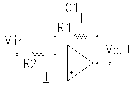
The configuration of the inverting amplifier is shown in Figure 1.

Figure 1. The inverting amplifier
The input-output relationship is derived as follows:

We implemented the circuit on a breadboard using R 1 = 30kΩ and R 2 = 10kΩ. We drove it with a 1kHz sine wave, that is 2V peak-to-peak. The expected gain was -3 and we verified this by observing the input and output using the oscilloscope. Figure 2 shows the input output relationship.

Figure 2. Input output relationship of an inverting amplifier with Gain = -3.
As we increase the input, there’s a point where distortion starts to appear because we cannot have infinite output. Figure 3 shows the maximum output swing (ie. The largest output we can get before distortion starts). The output swing is -11V, +11 V.

Figure 3. Maximum output swing.
We repeated the procedure with an inverting amplifier with R 1=10kΩ.
The expected gain was -1. and figure 4 verifies our expectations.

Figure 4. Gain of -1 with an inverting amplifier.
The maximum output swing doesn’t change as seen in Figure 5. you can see that the tips of the output signal are getting flat as the input signal crosses over ±11V.

Figure 5. Maximum output swing using a gain of -1.
Then we used a gain of -3 again to measure the slew rate (the maximum rate at which the output of the op-amp can change). Figure 6 shows the slew rate of 4V/µs. This does not agree with manufacturer’s specification of 15V/µs. We believe that the manufacturer considered the point at which the output signal crosses the desired output. In that case, our measurement shows that the slew rate is about 13V/µs but we think it is more honest to use the actual settling time.

Figure 6. Slew rate of 4V/µ s
2. non-inverting amplifier

Figure 7. non-inverting amplifier

In that case if we want to design a non-inverting amplifier with a gain of 11 we would choose the value of R 1/R 2 = 10. For instance, R 1=100kΩ and R 2=10kΩ would work.
We could also modify this to create a follower (an amplifier with a gain of 1) which is useful because we can create a buffer with it. It is useful for matching impedances between source and output voltages.
3. integrator

Figure 8. an integrator.

So, for a 2V peak-to-peak 1kHz square wave, the peak integrated value
Vo= -(500e-6 s * 1 V)/(100e3 Ω* 0.01e-6 F)=-500mV
so the peak to peak amplitude of the triangular wave output should be 500mV. In the lab, we measured a value of 580mV which compares well with our calculations. Figure 9, below, shows the output obtained in lab.

Figure 9. Output for the integrator circuit. The peak to peak voltage for the triangular wave output was measured to be 580mV.
4. the comparator

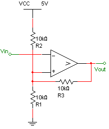
Figure 10. the comparator circuit.
The threshold voltage for this comparator is 2.5 V which means that if the input voltage is below 2.5V the output will be high (5V) and if it's greater, it will be low (0V). We can think that the op-amp has a switch at the end of it that allows it to provide two options as output. In the first case, the output is no voltage (ie, it's grounded, therefore we get current flowing but the Voltage appears to be 0). In the second case, we have no current; then if there's no current coming in the voltage drop across the resistor has to be 0 V meaning Vout is 5V. This is accomplished using R3 because it lets us make our 'no current' state a 'high voltage' state. Without it the output would be uncertain for inputs that are higher than 2.5 V. Figure 11 shows the output without the resistor and Figure 12 shows the effect of placing the resistor.

Figure 11. Uncertain output without the resistor.

Figure 12. Placing a resistor enables us to measure desired output.
5. the Schmitt trigger

Figure 13. the Schmitt Trigger.
To understand the Schmitt Trigger better, let's think about a noisy sine wave. Let's say that we're measuring daylight and we want to turn the lights on when it's dark and turn them off when it's light. If we use a symple comparator circuit, then at some time during the day, when we're crossing the threshold, our lights will turn on and off because of the slight variations in the input voltage and this is very undesirable. With the Schmitt Trigger, we can create two thresholds. When it becomes dark (the first threshold is overcome) then the second threshold dominates and if it becomes slightly lighter again, the lights won't turn off. They will only turn off in the morning when it's much lighter and then the first threshold will be in effect. This way, little perturbations will not cause our lights to flicker. Figure 12 illustrates the effect of the Schmitt trigger and compares it to a comparator circuit.

Figure 14. Schmitt Trigger vs Comparator.
6. relaxation oscillator
Let’s consider the case where V3 > V 2. The comparator would produce at the output, Vout = 0V. If Vout = 0V, then we can find V2 = 1.3V. Looking at the negative terminal now, we can see that because Vout = 0V, the capacitor will begin to discharge and as a result, V3 will decrease. If V3 drops below 1.3V or V2, then Vout will become high. In this case, if we consider the 1kΩ resistor to be much smaller than the other resistors in the circuit, we can assume that Vout ≈ 5V. Assuming Vout = 5V, we can easily find V2, which turns out to be V2 = 2.15V. Now looking at the negative terminal, we can see that the capacitor will charge if Vout = 5V. This will cause V3 to increase until V3 becomes larger than V2 = 2.15V, at which point the process will reverse and start again.
We can see this process easily on the oscilloscope. Figure 15 shows the circuit output. Ch1, which is monitoring V3, shows the voltage change associated with the charging and discharging of the capacitor. Ch2 monitors the positive terminal, or V2, and we can see that it changes states from 1.3V to 2.15V depending on the value of V3. When V3 dips below 1.3V, V2 becomes 2.15V and when V3 goes beyond 2.15V, V2 becomes 1.3V, although not instantaneously. Ch3 monitors the output of the comparator and we can see that Vout is high when V2 > V3 and Vout is low when V3 > V2.

Figure 15. Relaxation Oscillator
To derive the frequency of oscillation, we can simply consider the frequency of oscillation of the input at the negative terminal, since the output changes whenever V3 becomes greater than or less than V2. Hence, we can consider a simple RC circuit in which the capacitor, C1, and the resistor, R3, to be in series with Vout, which is either 5V or 0V. We can then analyze the circuit when the voltage across the capacitor, which is equal to V3, charges from 1.3V to 2.15V and discharges from 2.15V to 1.3V to find the frequency of oscillation.
V3 discharges from 2.15V to 1.3V.

V3 charges from 1.3V to 2.15V

Now that we have the time it takes for the capacitor to charge and discharge, we can calculate the resulting frequency of oscillation.

Looking at our measured result, we can see that the frequency of oscillation of channel 3, or Vout, is equal to 113.9 kHz. This value is close to our calculated value of 109kHz.
|